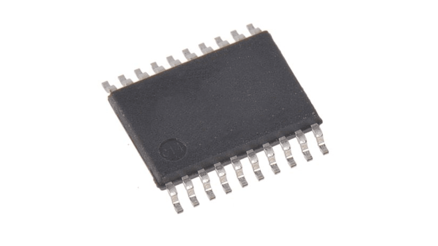
Renesas Electronics 5PB1110PGGI Clock Buffer 20-Pin TSSOP

- RS Stock No.:
- 254-4942
- Mfr. Part No.:
- 5PB1110PGGI
- Brand:
- Renesas Electronics
Available for back order.
Added
Price (ex. GST) Each (In a Tube of 74)
$7.256
(exc. GST)
$8.344
(inc. GST)
| Units | Per unit | Per Tube* |
| 74 - 222 | $7.256 | $536.944 |
| 296 - 444 | $6.616 | $489.584 |
| 518 + | $5.91 | $437.34 |
| *price indicative | ||
- RS Stock No.:
- 254-4942
- Mfr. Part No.:
- 5PB1110PGGI
- Brand:
- Renesas Electronics
Technical data sheets
Legislation and Compliance
Product Details
The Renesas Electronics high-performance LVCMOS clock buffer has an additive phase jitter of 50 fs RMS. There are five different fan-out variations available that is 1:2 to 1:10. Its supports a synchronous glitch-free output enable (OE) function to eliminate any potential intermediate incorrect output clock cycles when enabling or disabling outputs. It can operate from a 1.8 V to 3.3 V supply.
High-performance 1:2, 1:4, 1:6, 1:8, 1:10 LVCMOS clock buffer
Very low pin-to-pin skew: < 50 ps
Very low additive jitter: < 50 fs
Supply voltage: 1.8 V to 3.3 V
3.3 V tolerant input clock
fMAX is 200 MHz
Integrated serial termination for 50 Ω channel
Packaged in 8-, 14-, 16-, 20-pin TSSOP and as small as 2 x 2 mm DFN and 3 x 3 mm VFQFPN packages
Industrial (-40°C to +85°C) and extended (-40°C to +105°C) temperature ranges
For products that are Customized and under Non-cancellable & Non-returnable, Sales & Conditions apply.
Specifications
Attribute | Value |
|---|---|
| Maximum Supply Current | 27 mA |
| Maximum Input Frequency | 200MHz |
| Mounting Type | Surface Mount |
| Package Type | TSSOP |
| Pin Count | 20 |