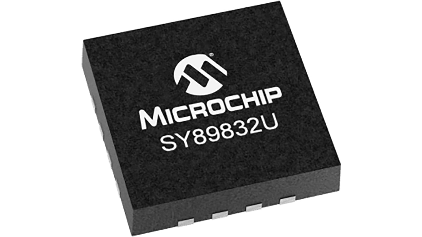
SY89832UMG, Clock Buffer LVDS, 1-Input, 16-Pin QFN
- RS Stock No.:
- 177-9675
- Mfr. Part No.:
- SY89832UMG
- Brand:
- Microchip

Currently unavailable
We don't know if this item will be back in stock, RS intend to remove it from our range soon.
- RS Stock No.:
- 177-9675
- Mfr. Part No.:
- SY89832UMG
- Brand:
- Microchip
Specifications
Technical data sheets
Legislation and Compliance
Product Details
Find similar products by selecting one or more attributes.
Select all | Attribute | Value |
|---|---|---|
| Brand | Microchip | |
| Logic Family | LVDS | |
| Logic Function | Clock Buffer | |
| Input Signal Type | Differential | |
| Output Logic Level | LVDS | |
| Operation Mode | Differential | |
| Number of Clock Inputs | 1 | |
| Mounting Type | Surface Mount | |
| Package Type | QFN | |
| Pin Count | 16 | |
| Dimensions | 3 x 3 x 0.8mm | |
| Length | 3mm | |
| Width | 3mm | |
| Height | 0.8mm | |
| Maximum Operating Supply Voltage | 2.62 V | |
| Maximum Operating Temperature | +85 °C | |
| Minimum Output Frequency | 2GHz | |
| Maximum Output Frequency | 2.5GHz | |
| Minimum Operating Temperature | -40 °C | |
| Number of Outputs | 4 | |
| Minimum Operating Supply Voltage | 2.37 V | |
| Select all | ||
|---|---|---|
Brand Microchip | ||
Logic Family LVDS | ||
Logic Function Clock Buffer | ||
Input Signal Type Differential | ||
Output Logic Level LVDS | ||
Operation Mode Differential | ||
Number of Clock Inputs 1 | ||
Mounting Type Surface Mount | ||
Package Type QFN | ||
Pin Count 16 | ||
Dimensions 3 x 3 x 0.8mm | ||
Length 3mm | ||
Width 3mm | ||
Height 0.8mm | ||
Maximum Operating Supply Voltage 2.62 V | ||
Maximum Operating Temperature +85 °C | ||
Minimum Output Frequency 2GHz | ||
Maximum Output Frequency 2.5GHz | ||
Minimum Operating Temperature -40 °C | ||
Number of Outputs 4 | ||
Minimum Operating Supply Voltage 2.37 V | ||
- COO (Country of Origin):
- US
The SY89832U is a 2.5V, high-speed, 2GHz differential LVDS (Low Voltage Differential Swing) 1:4 fanout buffer optimized for ultra-low skew applications. Within device skew is guaranteed to be less than 20ps over supply voltage and temperature. The differential input buffer has a unique internal termination design that allows access to the termination network through a VT pin.
Guaranteed AC performance over temperature and voltage:
DC-to >2.0GHz throughput
<570ps propagation delay (IN-to-Q)
<20ps within-device skew
<200ps rise/fall time
Ultra-low jitter design:
81fsRMS phase jitter
Unique, patent-pending input termination and VT pin accepts DC- and AC-coupled inputs
High-speed LVDS outputs
2.5V voltage supply operation
Industrial temperature range: -40°C to +85°C
Available in 16-pin (3mm x 3mm) QFN package
