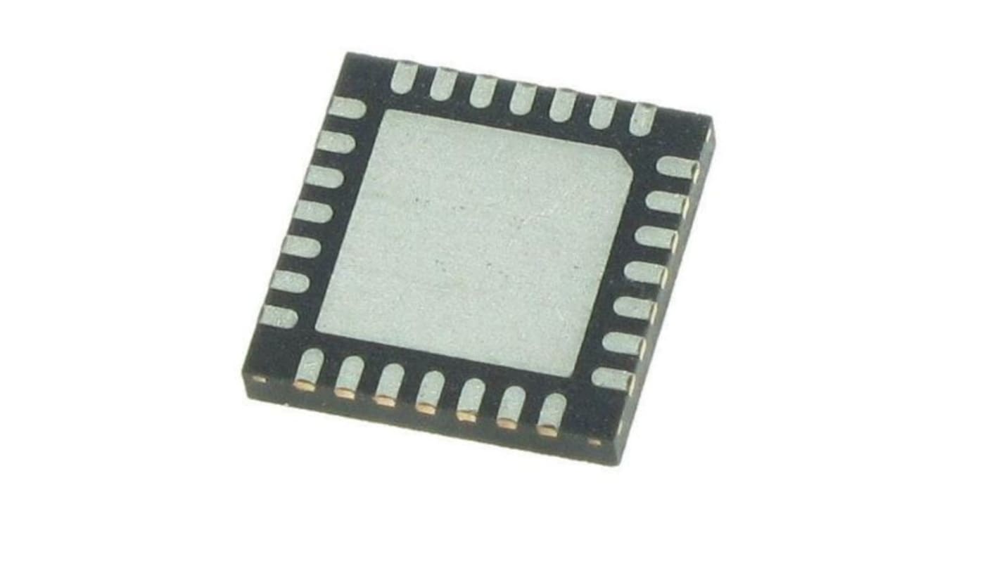
Renesas Electronics 8SLVP1208ANBGI Clock Buffer, 28-Pin LFCSP
- RS Stock No.:
- 216-6233P
- Mfr. Part No.:
- 8SLVP1208ANBGI
- Brand:
- Renesas Electronics

Bulk discount available
Subtotal 123 units (supplied in a tray)*
$2,001.21
(exc. GST)
$2,301.33
(inc. GST)
FREE delivery for orders over $60.00 ex GST
Stock information currently inaccessible
Units | Per unit |
|---|---|
| 123 - 244 | $16.27 |
| 245 + | $15.98 |
*price indicative
- RS Stock No.:
- 216-6233P
- Mfr. Part No.:
- 8SLVP1208ANBGI
- Brand:
- Renesas Electronics
Specifications
Technical data sheets
Legislation and Compliance
Product Details
Find similar products by selecting one or more attributes.
Select all | Attribute | Value |
|---|---|---|
| Brand | Renesas Electronics | |
| Product Type | Clock Buffer | |
| Mount Type | Surface | |
| Package Type | LFCSP | |
| Minimum Supply Voltage | 2.5V | |
| Pin Count | 28 | |
| Maximum Supply Voltage | 3.3V | |
| Minimum Operating Temperature | -40°C | |
| Maximum Operating Temperature | 85°C | |
| Standards/Approvals | No | |
| Width | 5 mm | |
| Length | 5mm | |
| Height | 0.7mm | |
| Series | 8SLVP1208 | |
| Automotive Standard | No | |
| Select all | ||
|---|---|---|
Brand Renesas Electronics | ||
Product Type Clock Buffer | ||
Mount Type Surface | ||
Package Type LFCSP | ||
Minimum Supply Voltage 2.5V | ||
Pin Count 28 | ||
Maximum Supply Voltage 3.3V | ||
Minimum Operating Temperature -40°C | ||
Maximum Operating Temperature 85°C | ||
Standards/Approvals No | ||
Width 5 mm | ||
Length 5mm | ||
Height 0.7mm | ||
Series 8SLVP1208 | ||
Automotive Standard No | ||
The Renesas Electronics 8SLVP1208 is a high-performance differential LVPECL fanout buffer. The device is designed for the fanout of high-frequency, very low additive phase-noise clock and data signals. The 8SLVP1208 is characterized to operate from a 3.3V and 2.5V power supply. Guaranteed output-to-output and part-to-part skew characteristics make the 8SLVP1208 ideal for those clock distribution applications demanding well-defined performance and repeatability.
Eight low skew, low additive jitter LVPECL output pairs
Two selectable, differential clock input pairs
Differential pairs can accept the following differential input
levels: LVDS, LVPECL, CML
Maximum input clock frequency: 2GHz
LVCMOS interface levels for the control input (input select)
Output skew: 28ps (typical)
Propagation delay: 410ps (maximum)
Low additive phase jitter, RMS: 54.1fs (maximum)
(fREF = 156.25MHz, VPP = 1V, 12kHz - 20MHz)