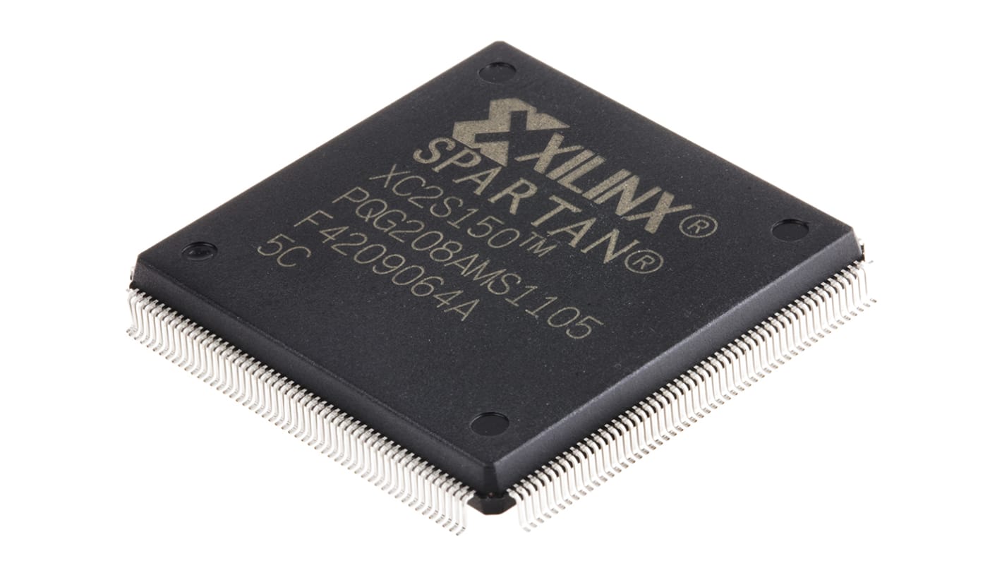
Xilinx FPGA XC2S150-5PQG208C, Spartan-II 3888 Cells, 150000 Gates, 55296bit, 864 Blocks, 208-Pin PQFP
- RS Stock No.:
- 626-0450P
- Mfr. Part No.:
- XC2S150-5PQG208C
- Brand:
- Xilinx

Unavailable
RS will no longer stock this product.
- RS Stock No.:
- 626-0450P
- Mfr. Part No.:
- XC2S150-5PQG208C
- Brand:
- Xilinx
Specifications
Technical data sheets
Legislation and Compliance
Find similar products by selecting one or more attributes.
Select all | Attribute | Value |
|---|---|---|
| Brand | Xilinx | |
| Family Name | Spartan-II | |
| Number of Logic Gates | 150000 | |
| Number of Logic Cells | 3888 | |
| Number of Logic Units | 864 | |
| Mounting Type | Surface Mount | |
| Package Type | PQFP | |
| Pin Count | 208 | |
| Number of RAM Bits | 55296bit | |
| Dimensions | 28 x 28 x 3.4mm | |
| Height | 3.4mm | |
| Length | 28mm | |
| Minimum Operating Temperature | 0 °C | |
| Minimum Operating Supply Voltage | 2.375 V | |
| Width | 28mm | |
| Maximum Operating Supply Voltage | 2.625 V | |
| Maximum Operating Temperature | +85 °C | |
| Select all | ||
|---|---|---|
Brand Xilinx | ||
Family Name Spartan-II | ||
Number of Logic Gates 150000 | ||
Number of Logic Cells 3888 | ||
Number of Logic Units 864 | ||
Mounting Type Surface Mount | ||
Package Type PQFP | ||
Pin Count 208 | ||
Number of RAM Bits 55296bit | ||
Dimensions 28 x 28 x 3.4mm | ||
Height 3.4mm | ||
Length 28mm | ||
Minimum Operating Temperature 0 °C | ||
Minimum Operating Supply Voltage 2.375 V | ||
Width 28mm | ||
Maximum Operating Supply Voltage 2.625 V | ||
Maximum Operating Temperature +85 °C | ||
- COO (Country of Origin):
- US
Related links
- Altera FPGA Cyclone II 4608 Cells 208-Pin PQFP
- Altera FPGA EP2C8Q208C8N Cyclone II 8256 Cells 208-Pin PQFP
- Digilent 410-376 Xilinx Spartan-7 Development Board ADC1410 for XC7S25 Spartan-7
- Digilent 410-352 Xilinx Spartan-7 Development Board ADC1410 for Hobbyists Makers
- Digilent Development Board AMD Spartan-6 XC6SLX150 FPGA Development Module 6 GHz 6002-410-047
- Digilent Development Board AMD Spartan-6 XC6SLX150 FPGA Software Defined Radio Development Module for USRP Hardware
- Xilinx XC2C256-7VQG100C 80 I/O ISP, 100-Pin VTQFP
- Microchip SAM9260 Microcontroller 8kB FLASH, 208-Pin PQFP